Artificial twisted-crystalline structures created at the IKZ
Novel complex crystal structures expand the possibilities of modern materials science
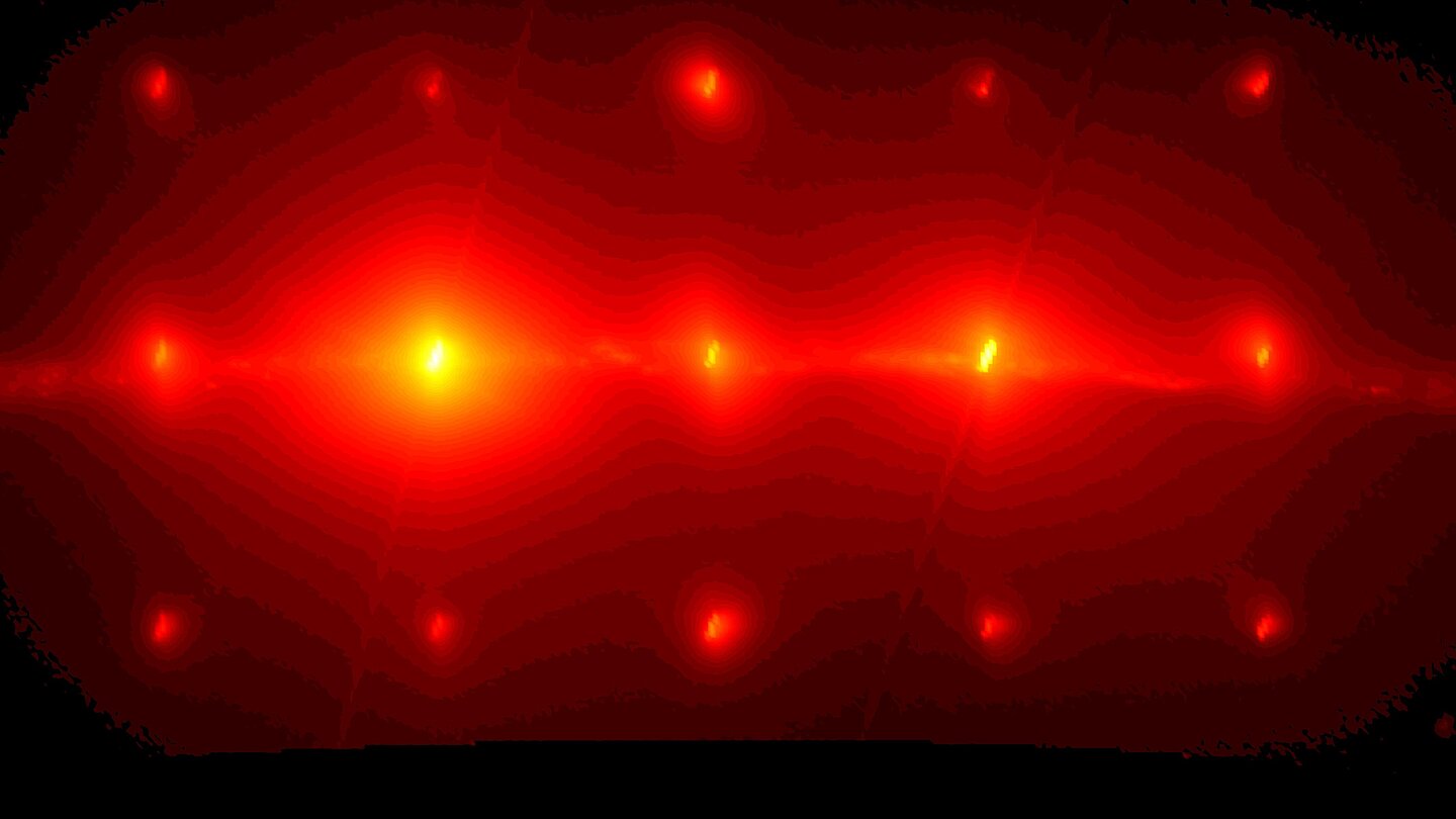
Novel complex crystal structures beyond what could be grown with traditional methods can be created using layer transfer. This applies in particular to twisted crystalline oxide structures. The microscopic structure of the twisted crystals is examined in detail using synchrotron radiation revealing the crystalline super-lattice as an array of diffraction spots. This technology enables new material properties and expands the possibilities of modern materials science.
Modern device applications demand increasingly advanced functional materials. Crystalline materials stand out via their highly regular arrangement of atomic building blocks constituting best performance materials for many applications. Technological crystals come in the form of bulk crystals or thin epitaxial layers.
At Leibniz-Institut für Kristallzüchtung (IKZ), bulk crystals are grown for specific applications such as solid-state lasers, high temperature piezo-electrics and single-crystalline substrates required for subsequent heteroepitaxial thin-film depositions from which the final devices for high performance micro-electronics are produced.
As a second column of crystal growth, IKZ conducts heteroepitaxy referring to thin film growth where the grown film inherits the crystalline orientation of the single crystalline substrate. Typical thicknesses of the deposited films range from few nanometers up to few micrometers. In epitaxy, additional concepts to manipulate materials properties can be exploited which are not accessible in bulk-growth. For example, strain engineering of thin films can be used to break the original crystal symmetry and for example to yield ferroelectricity. Another possibility is to create vertical superlattices, i.e. multilayer-structures with multiple repeated layer sequence such as A-B-A-B… These so-called vertical superlattices offer an enhanced parameter space for tuning material properties and for producing emerging effects such as “polar” vortices.
As a third column of crystal growth, IKZ has recently introduced the “2D goes 3D” strategy based on the transfer and stacking of crystalline layers. By doing so, subsequent layers are not grown on top of pre-existing ones, instead they are transferred as separately produced freestanding layer. Layer transfer overcomes certain constraints in heteroepitaxy such as the requirement of fitting lattice parameter and symmetry, or other thermodynamic or kinetic constraints such as the required growth temperature. Hence, new opportunities arise to create artificial crystalline structures via layer bonding.
Stacking of freestanding membranes enables the formation of interfaces beyond what can be obtained with classical heteroepitaxy. In particular, twisted interfaces generate Moiré-materials establishing a lateral crystalline superlattice and promising novel physical properties not existent in the corresponding individual layers. Moiré-materials constitute a novel class of material interfaces in which (opto-)electronic properties are tuned by the relative twist angle of the adjacent crystalline surfaces. For two-dimensional (2D) van der Waals materials, with graphene as its most prominent example, Moiré-materials are exploited for band structure engineering enabling correlated electronic phases. In 2D-van der Waals materials, the relatively weak interlayer interaction renders strain and structural relaxation a minor role, relevant mostly in the limit of small twist angles. This is different when considering oxide-based perovskites such as SrTiO3 with strong bonding across layers. In this case, structural reconstructions and their associated strain fields are crucial. Freestanding oxide perovskites are made available via the sacrificial layer approach opening a pathway towards oxide-based Moiré-materials.
In the limit of strong interaction across the interface, a twisted interface can be described by an ideal twist boundary resulting in an in-plane screw-dislocation network. Dislocations are linear crystalline structures within the crystal which possess a different atomic structure than the surrounding crystal. Hence, dislocations are often termed “defects” even though they could offer new functionality to the host crystal. Similarly, as in the case of Moiré-materials, the distance between dislocation lines is set by the twist angle between the adjacent crystalline surfaces (and the lattice mismatch in case that different materials are placed together). The associated strain gradients of the periodic pattern are especially appealing for oxide-based perovskites due to the intricate connection between surface polarization and subtle structural deformations such as the oxygen octahedra tilt.
Within DFG-project “nano-twist”, IKZ developed a transfer bonding process which produces efficient bonding of freestanding SrTiO3 layers to SrTiO3 single-crystal substrates. The integrity of the nm-thin layer is maintained by initially conducting a wafer-bonding process at high temperature and only subsequently dissolving the sacrificial layer.
The twisted SrTiO3/SrTiO3 interface is investigated by X-ray diffraction in grazing incidence geometry enabling the observation of clear signatures of a highly periodic lateral superlattice consistent with the formation of a screw-dislocation network. This work demonstrates a robust route for the fabrication of twisted perovskites and their development into a functional material platform with designed strain gradients at the nanoscale.
Twisted perovskites are just a first example of the novel IKZ “2D goes 3D” strategy to produce artificial crystalline structures via the layer transfer approach. In future, we will further expand this topic to other materials and material combinations.
We thank PDI for collaboration on the Pharao-Beamline (BESSY II), PETRA III (DESY Hamburg) for beamtime P08 (R-20241264) and ESRF for beamtime (experiment HC-5796), as well as the DFG for funding “nano-twist” MA 9075/1-1, SCHW 1500/9-1 and the European Regional Development Fund ERDF (project number 1.8 /15).
Contact:
Dr. Jens Martin
Leibniz-Institut für Kristallzüchtung (IKZ)
+49 30 246499-301
jens.martin(at)ikz-berlin.de
www.ikz-berlin.de
Press release IKZ, 11 March 2025