Innovation cluster for microsystems technology and materials in Berlin Adlershof
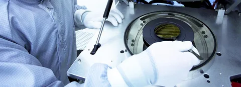
Microsystems technology (MEMS, or MOEMS) is an essential foundation for innovative products. Communications devices, medical technology and mobility are not conceivable without it. New materials like sensitive hydrogels, new nanocomposite and shape memory materials – ‘smart’ materials – facilitate complex systems comprising more functions in ever smaller components. The standard product supply chain involves semiconductor technology, MEMS (microelectro-mechanical systems), advance electronics packaging (including bonding technology), calibration and system integration.
Numerous businesses operating in this field are located at Adlershof, including Astro- und Feinwerktechnik Adlershof, FMB Feinwerk- und Messtechnik, FUSS-EMV and the German Association for Non-destructive Testing (Deutsche Gesellschaft für zerstörungsfreie Prüfung, DGzfP). Research institutes such as the Helmholtz Centre for Materials and Energy (Helmholtz-Zentrum Berlin für Materialien und Energie), the Leibniz Institute for Crystal Growth (Leibniz-Institut für Kristallzüchtung, IKZ), the Federal Institute for Materials Research and Testing (Bundesanstalt für Materialforschung und -prüfung, BAM), and the Ferdinand-Braun-Institute (FBH) are based here.

Space aplenty at the Centre for Microsystems Technology and Materials
The Centre for Microsystems Technology and Materials on Max-Planck Street spans 6,500 square metres. It includes cleanrooms, offices, physico-chemical labs and storage. Find out more about rental opportunities here.

The Adlershof Technology Centres were largely financed with funding from the GRW — Joint Task of Improving Regional Economic Structure and from the European Regional Development Fund (ERDF).