Machine learning helps improving photonic applications:
Photonic nanostructures can be used for many applications, not just in solar cells, but also in optical sensors for cancer markers or other biomolecules, for example. A team at HZB using computer simulations and…
Rough optics, smooth surface:
Thin-film solar cells made of crystalline silicon are inexpensive and achieve efficiencies of a good 14 percent. However, they could do even better if their shiny surfaces reflected less light. A team led by Prof.…
A Bavarian start-up teamed up with a Berlin-based energy provider on a project towards the digitisation of district heating data:
The “A² Adlershof Accelerator-Programm Berlin” made it possible for a Bavarian start-up and a Berlin-based energy provider to come together to work on a project towards the digitisation of district heating data. A²…
Helmholtz-Zentrum Berlin and partners want to further improve the manufacturing process:
HZB participates in a new consortium for Perovskite solar technology that is led by Oxford PV Germany GmbH. The consortium is funded by the German Ministry of Economics and Energy with 2.8 Million Euros and aims to…
Humboldt-Universität zu Berlin and Helmholtz-Zentrum Berlin form a joint lab and research group “Generative production processes for hybrid components”:
Solar cells, LEDs and detectors made of organic and hybrid semiconductors can nowadays be simply printed out, even together with teensy nanostructures that make them function better. The development of low-cost…
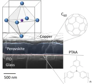
In perovskite solar cells, charge carriers are mainly lost through recombination occurring at interface defect sites. :
In contrast, recombination at defect sites within the perovskite layer does not limit the performance of the solar cells at present. Teams from the University of Potsdam and the Helmholtz-Zentrum Berlin (HZB) were…
Coordinator of the competence area “Crystal Growth Technology” at the Leibniz Institute for Crystal Growth (IKZ):
Peter Rudolph is the coordinator of the competence area “Crystal Growth Technology” at the Leibniz Institute for Crystal Growth (IKZ) in Berlin-Adlershof. Peter Rudolph (who got his degree as Electrical Engineer at…